Saturday, April 22, 2017

4/11 Temperature Measurement System Design & Wheatstone Bridge Circuits

We talked about cascaded op amp circuits.
A cascade connection is a head-to-tail arrangement of two or more op amp circuits such that the output of one is the input of the next.
We did a example of cascaded op amp circuit below:
We could see the circuit as two separate circuit and solve it by cutting it half.
 After this example, we did the lab.

Temperature Measurement System Design

In order to have a voltage output greater than 2, we need to find R1 and R2 that satisfy this situation, so we pick R1 to be 10k ohms and R2 to be 56k ohms.
In this lab, there were two parts. One is Wheatstone bridge design, and another is difference amplifier design.
The circuit below was our design of this lab.
The actual values of resistance are next to the resistor symbols.
The picture below is the basic set up for Wheatstone bridge design.
By balancing the bridge, we got the voltage across the thermistor to be 0V at room temperature like the picture shown below.
And this is the video that show the bridge working:
At room temperature, the voltage across the thermistor is 0V, and at body temperature, the voltage across the thermistor is 1.05V.

Next step, we connected Wheatstone bridge to a difference amplifier to produce a voltage output greater than 2V.
The video below shows that the entire system working:
From the video, we could see that the range of voltage output is from 0V to 4.12V, which satisfies the result what we expected the circuit to have.
By designing this circuit, we can make the output voltage whatever we want by easily changing R1 and R2.

After the lab, we leaned Instrumentation Amplifiers, which is the most useful and versatile op amp circuits for precision measurement and process control.
The voltage output follows the equation below:
 
The instrumentation amplifier is an extension of the difference amplifier in that it amplifies the difference between its input signals.

Summary
We leaned how to set up a temperature measurement system and how to balance Wheatstone bridge. Also, we learned a new amplifier, called Instrumentation Amplifiers. By learning these amplifiers, we can easily change the original voltage input to any output voltage we want.

Sunday, April 9, 2017

4/6 Summing Amplifier & Difference Amplifier

We learned many other amplifiers today.
We started with the unity gain buffer amplifier.

We did a example to calculate the Vo if Vs = 0 in the circuit above.
By using nodal analysis, we got Vo = -1.6364V.
And then, we talked about Non-inverting Amplifier which is an op amp circuit designed to provide a positive voltage gain.
The relationship between Vin and Vout of non-inverting amplifier is:

Next, we talked about Summing Amplifier.
The relationship between Vin and Vout of summing amplifier is:
indicating that the output voltage is the sum of the inputs. 
Then, we did lab.

Summing Amplifier
The picture above is the basic set up for this lab.
In this lab, the relationship between Vin and Vout is:
The actual resistance of R1=6.71k ohms
R2=6.67k ohms
R3=6.73k ohms
We got the following table and graph.
The data matched the equation.
For Va=3V and 5V, Vout is at saturation.
The picture is the calculated data we expected to get, but the maximum Vout we could get is 5V and -5V, so we can only get the Vout up to -3.44V.

After summing amplifier lab, we talked about Difference Amplifier.
The relationship between Vin and Vout is:
the amplifier must have the property that Vo = 0 when  V1 = V2 . This property exists when
so we can get:
Difference Amplifier
The picture above is the basic set up for this lab.
The relationship between the input and output voltages we determined in the class is the picture below.
The actual resistance of R1=9.94k ohms, R2=19.9k ohms, R3=9.98k ohms, and R4=19.7k ohms.
The table above is when we set Vb=1V, and vary Va.
We got the graph below:
From the data we got, it followed the relationship between the input and output voltages we determined in the class. 
For Va=-4V, -2V, 3V and 5V, Vout is at saturation.

After this lab, we ended up with analyzing a circuit below:
 
This is a non-inverting amplifier circuit.
By using nodal analysis, we can get the relationship between VL and VT.

Summary
We learned about Non-inverting Amplifier, Summing Amplifier, and Difference Amplifier today. By doing the lab, we knew how each amplifier works and what are the differences between different amplifiers. Each amplifier works differently in the circuit, and the relationship between the input and output voltages are different, too. Next class we will learn more amplifiers which are called differentiation and integration amplifiers.

4/4 Inverting Voltage Amplifier

I was taking the exam today, so I missed the lecture.
We learned about operational amplifiers which perform mathematical operations of addition, subtraction, multiplication, division, differentiation, and integration.
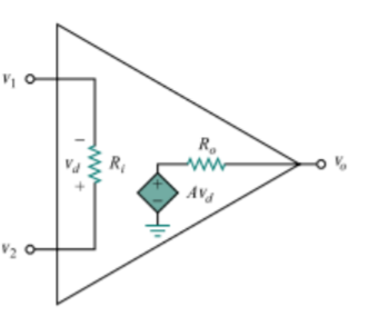
The op amp is an electronic unit that behaves like a voltage-controlled voltage source.


We leaned how to transfer it into a circuit. The picture above is how we view it in a circuit.
When the time I finished the exam, the class was doing the lab.

Inverting Voltage Amplifier
The picture above is the basic set up for this lab. 
If we redrew the circuit, we got the circuit above.
We chose the use 2.2k ohms and 4.7 ohms resistors to design an inverting amplifier which provides a gain of approximately 2.
We got the graph below:
 
The relationship between Vin and Vout for this circuit is: 
The dots in the middle of the graph follow the equation above.
From the first three dots and the last three dots of the graph, we can see that the Vout is at saturation.

Summary
We leaned how op amp works in a circuit and why do we need to use op amp in real life. We only learned one type of op amp today, which is inverting voltage amplifier. We will learn many different types of op amp in the future class. 

Monday, April 3, 2017

3/28 Thevenin's Theorem

We started with a circuit and used Everycircuit to find the value of the current through RL. The picture below was the circuit we drew in Everycircuit.


After that, we did a problem by using Thevenin's Theorem, but I forgot to take a picture...
Then we did out lab for today.

Thevenin’s Theorem


The picture above is the calculated Rth and Vth for this circuit. We got Rth = RL =7.7k ohms and Vth = 0.46V.
Resistance error:
1k(0.96k), 2.2k(2.15k), 4.7k(4.6k), 6.8k(6.68k), 1.8k(1.74k), 6.8k(6.68k)


The picture above is the basic set up for this lab without power supply.

The measured value for the Thevenin resistance is 7.4kohms, comparing to the calculated value (7.7kohms), the % error is 3.90%.
To measure the Thevenin voltage, we need to apply voltage source.

The picture above is the basic set up for the circuit with power supply.

The measured value for Thevenin voltage is 0.448V, comparing to the calculated value (0.46V), the % error is 2.60%.

For part three, we chose a 4.5k ohms resistor as our load resistor, and we calculated that the voltage across the load will be 0.187V.
From our measurement, we got 0.165V. The % error is 11%.
The reason why it is not very precise is because the value of the resistors are different than the actual values of the resistors.

For part four, we used the potentiometer to create the measured values of thevenin resistance (7.2ohms), and then, we supplied the circuit with 0.488V.
We used the same resistor that we used in part three (4.5k ohms) into the circuit, and we got the voltage drop is 0.167V, comparing this value to what we calculated, the % error is 1.1%.


The maximum resistance that the potentiometer can create is 8.5k ohms, so we cannot graph a bell curve that we expected.

Summary
We leaned about how to use Thevenin's Theorem and how to apply it to a real circuit. The lab proves that Thevenin's Theorem is a pretty uesful tool to analyze the circuit and to create a much simpler circuit that has the same function. Also, we knew how to find the maximum power dissipated by the load when the RL=Rth. 

3/23 Superposition II

Today, we leaned a new method to solve big and complex circuit, which is called linearity and superposition.
To me, I feel it is not my favorite way to solve a circuit.

The picture above is linearity problem. From the picture, we knew that if we doubled the Vs, the current i0 is doubled because of the linearity property.
After the linearity problem, we did our lab.

Superposition II


To use superposition, we need to follow these steps.
1. Turn off all independent sources except one source. Find the output (voltage or current) due to that active source using nodal or mesh analysis.
2. Repeat step 1 for each of the other independent sources.
3. Find the total contribution by adding algebraically all the contributions due to the independent sources.
(From Day 7 Notes Superposition and Source Transformation)

From the picture, we coverd the 5V voltage source first, and we got the voltage across 6.8k ohms resistor is 0.708V. Next, we covered the 3V voltage source, and we got the voltage across 6.8k ohms resistor is 1.99V. We added these two numbers together, and we got the final answer of the voltage across 6.8k ohms resistor = 2.698V.
Resistor Error:
9.8k(10k), 4.6k(4.7k), 0.975k(1k), 6.5k(6.8k), 21.7k(22k)

The picture above is the basic set up for this lab.

The picture above was when we took off the 5V voltage source, we got the voltage across 6.8k ohms resistor was 0.693V.

The picture above was when we took off the 3V voltage source, we got the voltage across 6.8k ohms resistor was 1.97V.

The picture above was when both 5V and 3V were active, we got the voltage across 6.8k ohms resistor was 2.66V.


The picture above is the summary of this lab. The % difference for each value are all less than 3%, which is very low, and this proves that superposition works.

Summary
We leaned how to use linearity and superposition today. To me, I feel superposition involved more work and it takes more time to solve one question. Maybe there are some of the questions that are easier to solve by using superposition, example: less power supply questions. But I will still use another method except superposition. haha

3/21 Mesh Analysis 2 & Time Varying Signal


We started with a circuit and used mesh analysis by applying KVL to solve this problem.

After this problem, we started our lab.

Mesh Analysis 2

First, we calculated the expected value for V1 and I1, and we got V1=5V and I1=-0.3224 mA.
Then, we set up the lab.

The picture above is the basic set up for this lab.

From the picture above, the measured value for V1 is 4.97V and the measured value for I1 is -0.321 mA.

From the analysis above, we calculated the % error for V1 = 0.6%
and the % error for I1 = 0.43%
From this experiment, we knew that mesh analysis worked really well.

After the lab, we did another problem about transistor.

The larger the transistor, the more heat it can take but more expensive.
We calculated the power out of the transistor is 4.266*10^-2 W, which lead us to use T092 transistor which matched what we needed.

After this problem, we did our second lab for today.
Time Varying Signal 

The picture above is the basic set up for this lab.
Picture 1:Sinusoidal wave 

Picture 2: Triangular Wave.

Picture 3: Square wave


Summary
We reviewed mesh analysis and applied it into the real circuit.
Then, we leaned how to choose and use transistor. The bigger the transistor, the more power input it can handle but more expensive, which means that to find the appropriate one is very important.

After that, we used wave form generator to create different shape of the voltage graph.